Start Up Fails When HDD Connected

I wonder if you'll get meaningful results with a 2.5 (laptop) drive? I thought I had read previously some people use a 2.5 drive when the motherboard can't support a 3.5 drive.
Yes, because a 2½" drive doesn't need 12V so can be driven from the USB port as an external drive. It's not particularly relevant whether the internal power could run it, my aim is to find out why it's not running a standard drive.

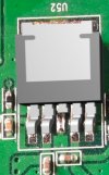
What I need to do now, with replacement parts on such long lead time, is (with courage) swap U52 with one from a working unit and see whether the problem switches place (at risk of busting both of them). There are several other parts on the main board with the same TO252-5 package, but they do not appear to be the same device. Edit: one is, it had its markings ground off on the board I happened to be looking at!
 
Last edited:
There is no apparent oscillation even at much shorter timebases.
There goes that idea. As you say it looks like it's being shut down - I take it you've looked at what's going on on the control pin (pin 1)?

As for the double edge, the decay rates match, so from here it's being enabled, shut(s) down, enabled, makes it to 5V OK then shut(s) down.

[Edit] I'll have a think and maybe a play sometime tomorrow.
 
I take it you've looked at what's going on on the control pin (pin 1)?
I had, and at first sight there was nothing obviously suspicious, but I have had another look:

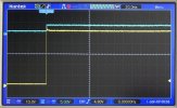
Here it is (blue trace) enabling the LDO without a HDD (sorry about the overlapping traces):
07F6E92B-B699-4CFF-9B8F-AAB7184B4F9B.jpeg

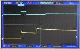
...and here it is with a load connected, enabling and then disabling after about 27ms (plenty of time for a processor to decide something is wrong and restart):
ABA5FAD4-BAAF-4B8B-8879-649D37208DAF.jpeg

The double ramp-up seems to be something to do with how U52 responds to the enable pin.

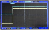
So then I had a look on a working HDR with load:
BBC2EB44-C82A-42E0-A09D-6DBAD12124E0.jpeg

On a much faster timebase, enable to output is about 500us (although the output starts ramping up within a few us).

I haven't changed the scale of the blue trace, only shifted it down so it fits on the screen! So the enable pin isn't being driven hard enough, maybe because the enable pin is bust and has gone low impedance. I'll have a fish around and see what else I can find, try to map out the circuit (tricky).
 
Last edited:
  • Like
Reactions: /df
So the enable pin isn't being driven hard enough, maybe because the enable pin is bust and has gone low impedance.
Fig 16 on the datasheet shows the control input cct. It's the base of an NPN transistor with a 27k/31k pot divider. Figure 13 gives a threshold somewhere around 1.5V which fits.
 
To summarise the current situation, there are two mysteries:
  1. Why the unit resets if 5V does not appear on the HDD power at the right time. This is unimportant, it just does.

  2. Why there is a runt signal on the enable (CTL) pin U52/1. This appears to be the crux of the matter, and the fact even a runt signal is able to turn the LDO on when there is no current demand (but not for higher current as is required with the load of an HDD) obscures the problem when just probing around with a meter. I think it's a property of the analogue (rather than digital) implementation of the device.
Thinking out loud: it is bothering me that the enable pin characteristics are only specified at zero load current. I presume the signal is supposed to be adequately buffered that the characteristics do not change significantly, so why not specify at a more useful load current (ie 1A)? If the pin is adequately buffered, why is there a difference in behaviour between load and no load? When the input transistor will be off for an enable pin voltage less than 0.8V max, why does the LDO appear to turn on (no load) with a runt input of 0.6V?

My speculation is that the 'scope traces are wrong or being misinterpreted. I think I might have had a bad contact (hand-holding the probe onto the pin, or maybe the probe grounding). The 'scope's vertical scale is not obvious: I'm using 10x probes, and I'm not sure whether the scale factor shown on-screen is per division or full scale (will clarify that point using the calibration signal). Whatever, my conclusion (that a runt signal results in a low-drive output) does not, on second thoughts, appear likely – especially considering the enable pin input structure.

I shall repeat the measurements and confirm what's what. If it really is a runt signal, why? Either the input has gone low impedance (not very likely) or the drive is broken (which I presume to be a general purpose I/O pin on the SoC). I should be able to determine which by lifting the enable pin (tricky but doable).

If I find, as I suspect, the signal is not a runt and the error is in measurement, I'm back to pinning the blame on the LDO being bust, with the series pass element gone high impedance (able to pass some current, but not enough to drive the load). This seems the most likely scenario to me, by principle of Occam's Razor.
 
Looking at the image in the OP, it looks like the control pin (pin 1) is being diven by a potential divider with a capacitor for filtering. Does probing the input to that and comparing it with a good unit provide any clues?

Edit, Deleted my earlier edit which was wrong.
 
Last edited:
I've been delving deeper, inspired by my waking thoughts.

First: the 'scope. It turns out I had the channels configured for x10 probes... but the probes are switchable x1/x10 and (you guessed it) I had them switched to x1! The calibration indicated at the bottom of the screenshots should be per division (sensible), but because of the config error the scale should be divided by 10.

Second: the runt pulse is a red herring - it reaches 2.9V at the pin (working or not). U52 is firmly in the frame.

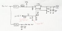
Here's a rough sketch of the overall layout and the details around U52:

1618231802300.jpeg

I tracked U52's input voltage to a coil and IC (which I presume to be a buck converter), using switch-mode to reduce 12V to a voltage just sufficient for the LDO and therefore minimising the wattage U52 has to dissipate.

What is more interesting is that the SMPS also feeds U53, another 00BC0W (despite what I said earlier – the board I happened to be looking at had the markings ground off). I probed around to find what U53 supplies, and it appears to be just two uncommitted socket positions (and associated components) nearby which look for all the world like unused USB ports! This gives me the idea that U53 might actually be spare.
 
What is not really clear from the datasheet is whether or not the package has a pad on the rear surface. If so it would normally be soldered onto an equivalent pad on the board with a good thermal connection to large area copper or ground planes within the board. If so, then the board would probably need preheating since it would be very difficult to remove. You might be lucky in that it could be just be the visible ground tab.
 
If it's like this, there's about 3 times more pad under the package than the exposed fin, which is functional Gnd (pin 3 is NC). S/t like this TO252-5-reverse.jpg
 
What is not really clear from the datasheet is whether or not the package has a pad on the rear surface.
I was looking at that too.

If so, then the board would probably need preheating since it would be very difficult to remove.
Ouch! Suck it and see. If I have trouble I'll make a mask (to protect surrounding components) and apply hot air. One can but try!

I have recovered components from a prototype SM board before now (because we had run short for the next prototype), with (effectively) a Black&Decker paint stripper and a sharp bang on the table!
 
This thread reinforces my belief that I need to stick to only attempting hardware fixes that can be accomplished using a screwdriver and hammer :)
 
Not gone through this properly - I'm in the middle of making sawdust - but the 8k2 is a pull-down to make sure the control pin is always low unless being driven high regardless of the power-on state of the device driving it. I'm guessing now, but although there are internal resistors to 0V in the regulator, there may be a time when the signal driving the control pin is goes tristate and they want to pull charge off the cap on the control pin quicker than the internal pulldown would.

[Edit] Or there's another load on the control line that has a weak pull-up.
 
Last edited:
My kingdom for some desoldering braid (I'm sure I have some somewhere, meanwhile eBay)... God I miss Maplin!
 
Last edited:
My kingdom for some desoldering braid (I'm sure I have some somewhere, meanwhile eBay)... God I miss Maplin!
My method would be to lift the legs one at a time then put a 6mm flat bit in the Weller TCP and deal with the tab.

FWIW before condemning the regulator I'd remove the 1k0 series resistor and drive the control pin independently to see what happens.
 
before condemning the regulator I'd remove the 1k0 series resistor and drive the control pin independently
Would you? Can't see any point (and I don't fancy my chances of getting that tiny grain-of-sand resistor back in place).

My method would be to lift the legs one at a time
Yes, but very carefully, and I still need the wick to flatten off the tab land before refitting.
 
Anyway, I'm on stop now until I lay my hands on some solder wick. A salvaged (or new) BA00BC0W has to go on flat.
 
Ah, sorry. I was forgetting it would be something like an 0402.
But it might be possible to desolder and lift just the control pin and improvise the necessary drive circuit (a small 1k resistor soldered to the control pin and connected to Fin for disable or VCC for enable?).
 
Back
Top